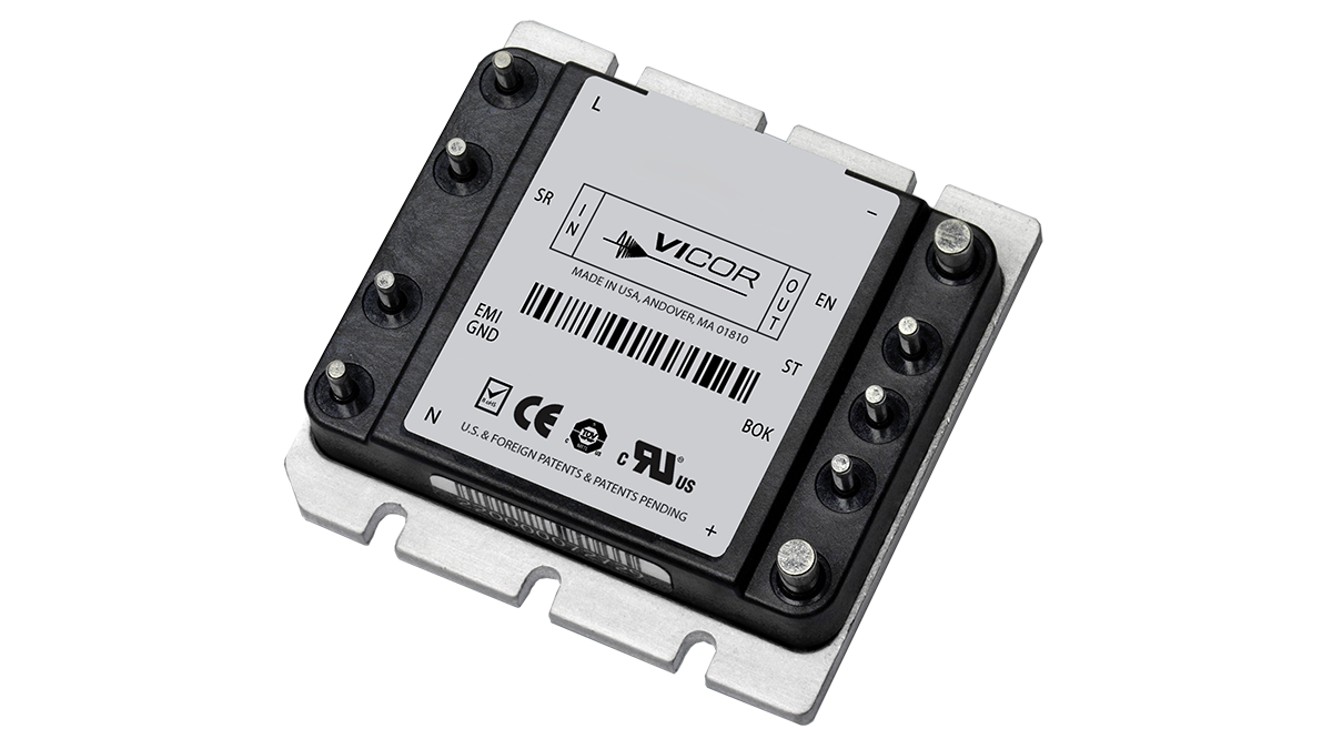
The Vicor FARM3HN1 is a sophisticated AC-to-DC front-end power stage module, purpose-built to simplify and optimize power system architecture. It masterfully integrates three crucial, high-performance functions:
Integrated EMI Filtering: Essential for meeting global regulatory standards by suppressing electromagnetic interference (EMI).
Autoranging Rectification: Automatically adapts to different worldwide AC input voltages, ensuring reliable operation across universal AC mains.
Robust Inrush Current Limiting: Protects the system and input components by managing the momentary surge of current during power-up.
This seamless integration allows the FARM3HN1 to connect directly to universal AC input lines globally. When paired with subsequent power components, specifically Vicor's 300V nominal DC-DC converters, this module enables the rapid deployment of a complete, automatically regulated, high-density, and low-profile switching power supply solution, dramatically streamlining the path to high-performance system design.
1. Test Circuit Diagram and Configuration
The validation tests for the FARM3HN1 were conducted using the reference design specified in Section 6 of the official Vicor datasheet (see accompanying image below). This standard configuration ensures that our results are directly comparable to the module's published specifications.
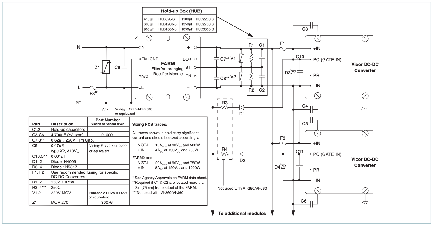
The core component under test—the Filter/Autoranging Rectifier Module (FARM3HN1)—is highlighted within the blue dashed box in the diagram.
We strictly adhered to the peripheral component values and circuit topology recommended by the manufacturer to accurately assess the module's performance in a typical application environment.
2. Rectification Functionality Test: Maximum Input Voltage 264 VAC
This test focused on validating the FARM3HN1's rectification performance under its maximum continuous input voltage and confirming the resulting DC output level.
Test Methodology and Observation
Input Condition: An AC input of 264 VAC was applied to the input terminals (labeled 'U' in the test setup image).
Measurement: The resulting DC output voltage (VDC) between the +OUT and -OUT terminals was measured.
Result: The measured output DC voltage was 365 VDC.
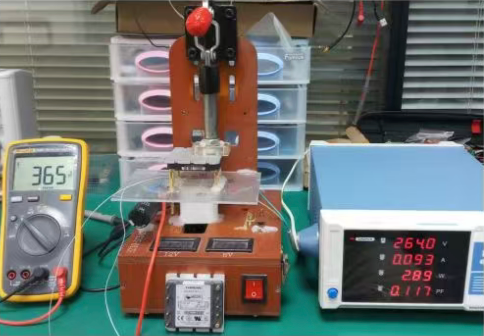
(Note: As shown in the image above, applying 264 VAC to port U resulted in a DC output of 365 V.)
Analysis and Compliance
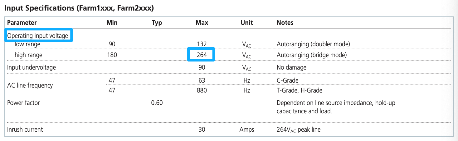
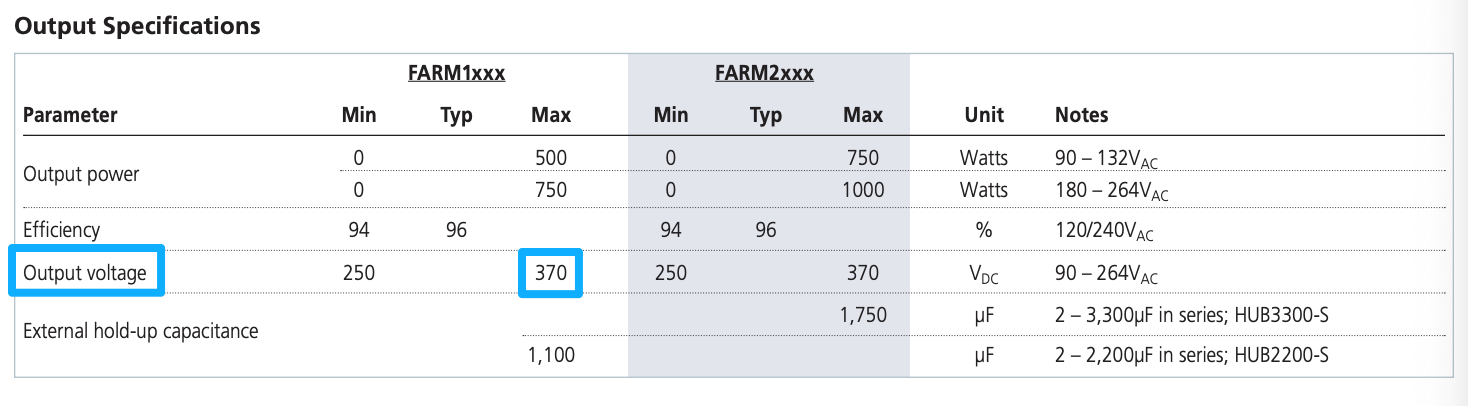
Since an official datasheet for the FARM3HN1 is not yet available, we referenced the specifications of the related Vicor FARM family (e.g., FARM1xx and FARM2xox series) as a benchmark.
The standard specification for the rectified DC bus voltage at 264 VAC input is typically capped at a maximum of 370 VDC.
Conclusion: The measured output voltage of 365 VDC falls well within the expected and permissible range (370 VDC or less). This successfully verifies the module's stable rectification functionality under the absolute maximum continuous AC input voltage of 264 VAC.
3. Rectification Functionality Test: Minimum Input Voltage 90 VAC
This segment validates the FARM3HN1's performance at the lower end of the universal AC input range, specifically 90 VAC, to ensure proper DC bus voltage delivery.
Test Methodology and Observation
Input Condition: An AC input of 90 VAC was applied to the Line (L) and Neutral (N) terminals.
Measurement: The DC output voltage (VDC) between the +OUT and -OUT terminals was measured.
Result: The measured DC output voltage was 246 VDC.
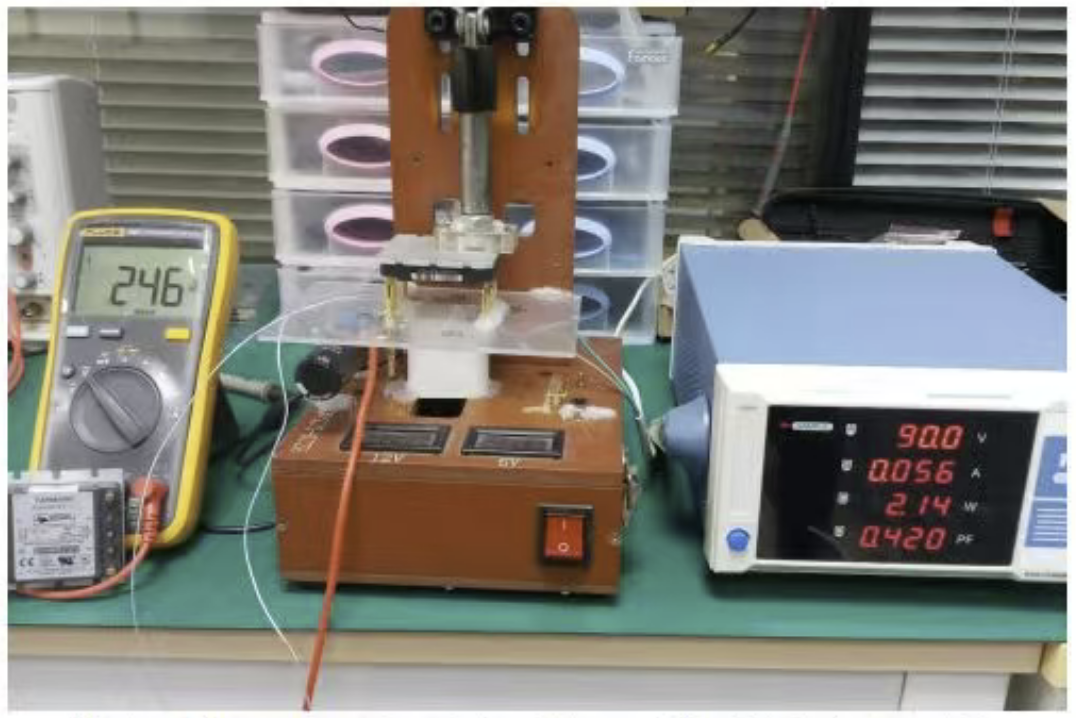
(Note: As depicted in the accompanying images, applying 90 VAC to the L/N ports resulted in a DC output of 246 VDC.)
Analysis and Performance Range
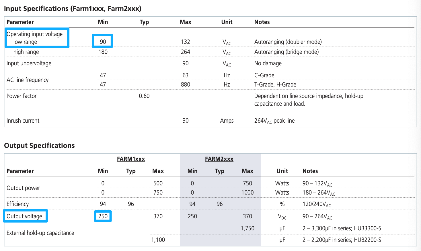
Consistent with the previous section, we referred to the specifications of the related Vicor FARM family (FARM1xxx and FARM2xxx) for comparative data, where the target minimum regulated VDC is often specified around 250 VDC at the low input boundary.
The measured 246 VDC is very close to the 250 VDC reference value. Further testing confirmed that the system achieves the target 250 VDC output when the AC input is slightly increased to approximately 91.8 VAC.
Conclusion: The module demonstrates the capability to maintain the DC bus voltage within the standard operational range, effectively covering the 250 VDC requirement at the lower end of the universal input voltage range. This confirms the robustness of the Autoranging feature.
4. Output Power Capability Validation
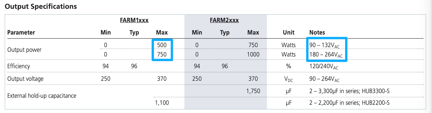
This crucial set of tests validates the FARM3HN1's power delivery capabilities across its specified operating voltage ranges. The module's performance is expected to conform to the power limits referenced in the official Vicor documentation, which define its load capacity based on the input voltage.
Vicor Reference Specifications (Power Derating)
 56【咯;=‘
As per Vicor's reference data for the FARM series (shown in the image below):
Test 4A: Low Line Maximum Power Verification (500 W)
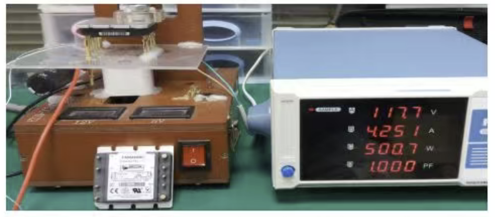
We tested the module's ability to drive a full load at the low end of the input voltage spectrum.
Conclusion: The tested output power successfully exceeded the 500 W specification for the low-line input range (90 VAC to 132 VAC). This result confirms compliance with the low-line power derating requirement.
Test 4B: High Line Maximum Power Verification (750 W)
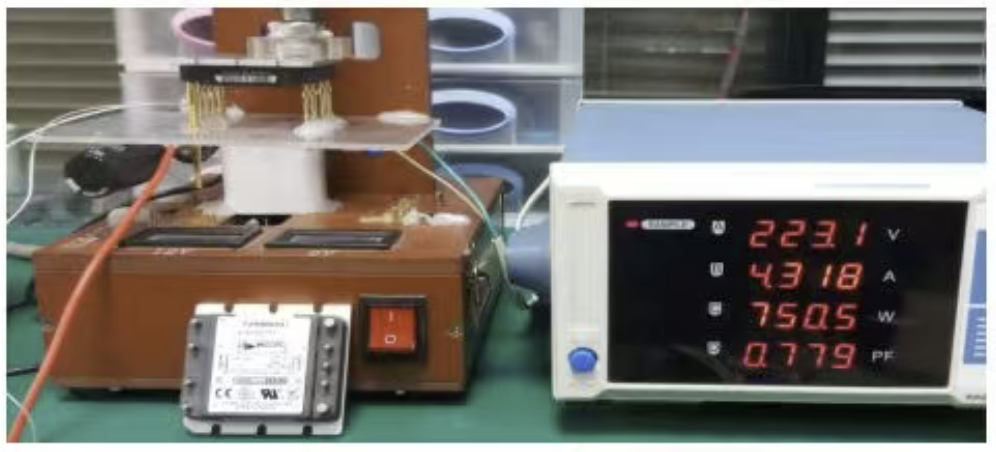
We tested the module's ability to drive its maximum rated load at a typical high-line input voltage.
Conclusion: The module reliably delivered its maximum rated continuous output of 750 W at the high-line input. This result satisfies the high-line power requirement (180 VAC to 264 VAC) and demonstrates the module's full-power capability.
5. Control Pin Timing and Internal Driver Voltage (EN, BOK, VCC)
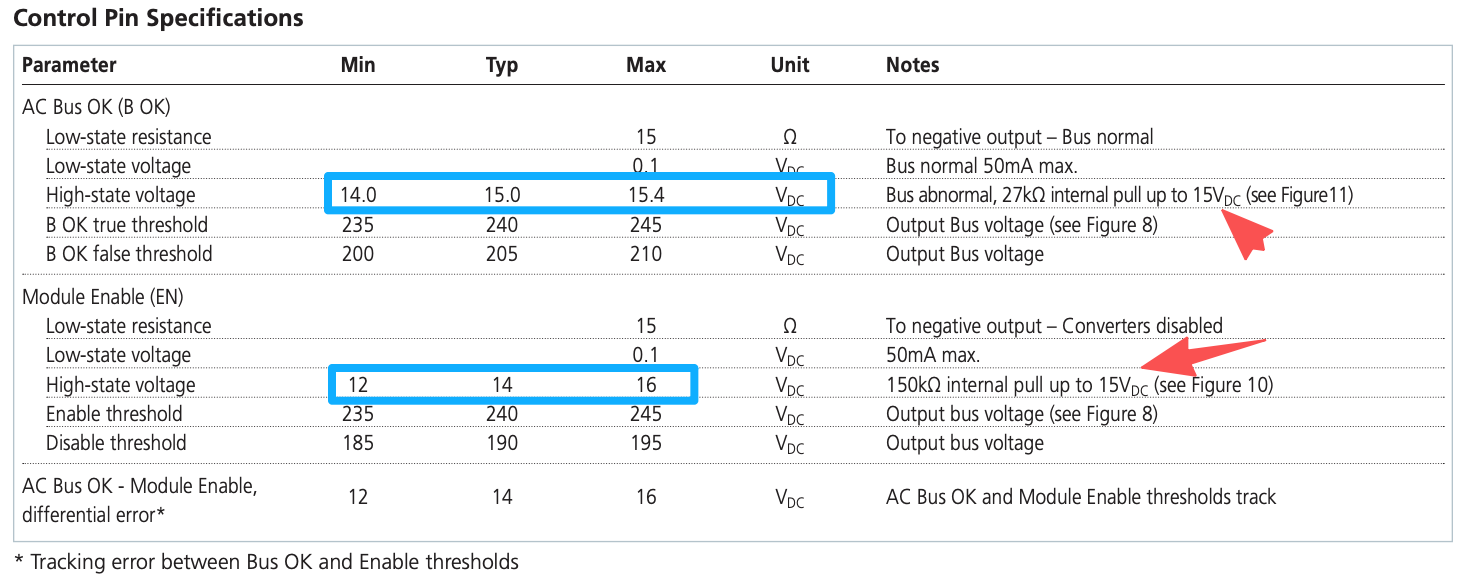
This section focuses on validating the transient control signals—specifically the Enable (EN) and DC Bus Good (BOK) pins—during power-up and power-down sequences, along with the internal logic supply voltage. Accurate signaling is essential for system-level control.
5A. Power-Up Timing Waveforms (EN and BOK)
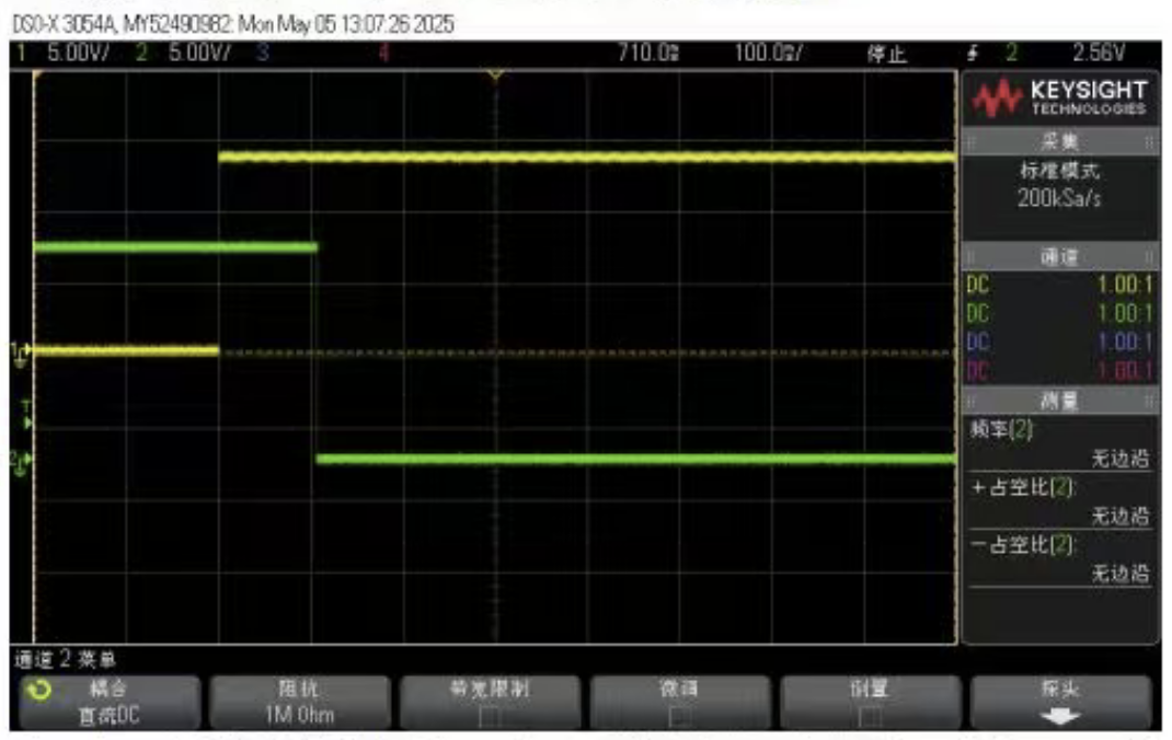
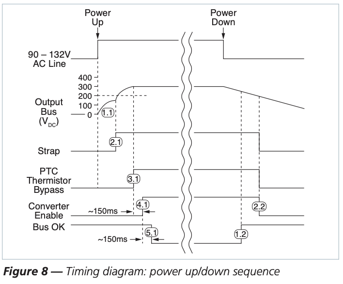
The images below show the output waveforms of the EN and BOK signals during the module's power-up sequence.
Observation: There is an approximate 100 ms delay between the assertion of the EN signal and the BOK signal becoming active.
Compliance: This observed timing is consistent with the reference timing diagrams provided in the related Vicor datasheets. While the 150 ms reference value is provided for guidance, the specifications do not mandate a precise minimum or maximum timing for this delay, making the 100 ms measurement acceptable.
5B. Internal Driver Voltage (VCC) Verification
We also measured the internal logic supply voltage (VCC) which drives the control circuitry.
Measurement: The measured VCC level was approximately 15 V (read as three divisions at 5V per division on the oscilloscope).
Compliance: This measured 15 V VCC level aligns directly with the reference data provided in the specification, confirming the internal supply is correctly regulated.
5C. Power-Down Timing Waveforms (EN and BOK)
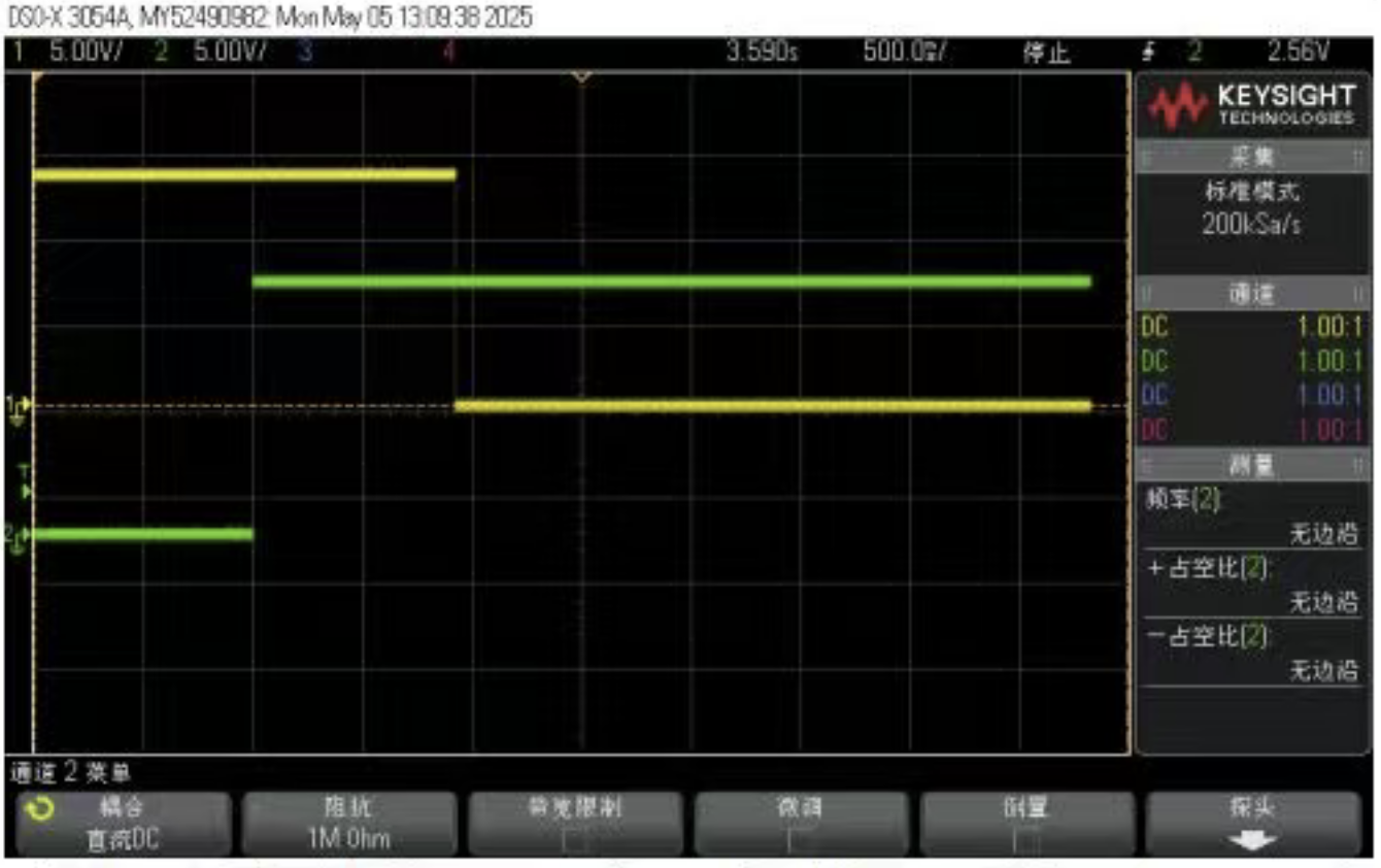
The images below show the waveforms of the EN and BOK signals during the module's power-down sequence.
Observation: The delay between the EN and BOK signal transitions during power-down was measured to be approximately 1,000 ms (1 second).
Compliance: Similar to the power-up sequence, this power-down timing is fundamentally compliant with the reference timing behavior, even though the datasheet does not specify a mandatory minimum or maximum timing value for this specific power-down delay.